AWG Architecture and Execution Timing
Global Architecture
The HDAWG Arbitrary Waveform Generator functionality is realized using field-programmable gate array (FPGA) technology. In order to provide sufficient digital signal processing resources to supply 4 or 8 high-speed outputs, the instrument architecture contains two types of FPGAs: 1 back end FPGA handling the central tasks of signal distribution and synchronization, and 2 (or 4) front end FPGAs, each feeding one pair of front panel Wave, Mark, and Trig connectors. This is sketched in Figure 1 for the 4-channel model HDAWG4, and an analogous diagram is valid for the HDAWG8.
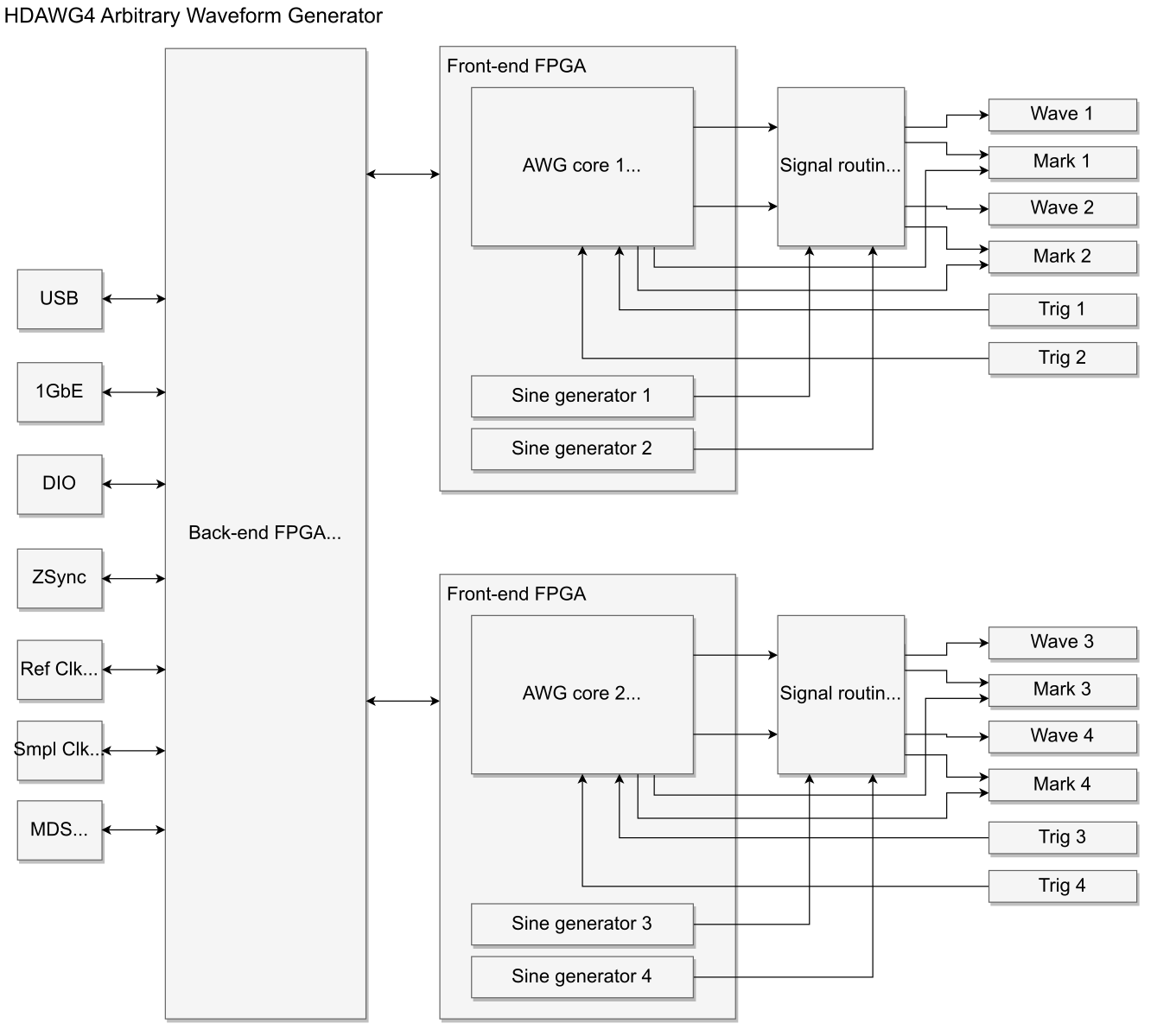
On each front end FPGA, there is one so-called AWG Core, which is the unit sending waveforms from the waveform memory to one pair of Wave and Mark outputs. Additionally, each front end FPGA holds 2 sine generators for digital modulation of this pair of outputs. This aspect of the HDAWG architecture is most relevant in understanding the channel grouping feature as well as triggering.
- Independently of the channel grouping mode of the HDAWG (1x8, 2x4, 4x2), sequence programs are always executed on the AWG cores. This means, e.g., in 1x8 mode, a high-level sequence program written in the AWG Sequencer Tab is getting compiled into 4 low-level sequence programs that are executed in parallel on the 4 AWG cores. The back-end FPGA synchronizes the execution timing.
- Sine generator signals are local within one front end FPGA, which is why combinations between AWG channels and sine generators for digital modulation are only possible within one output pair
- Oscillator signals are global with HDAWG-MF option, this is realized by having multiple synchronized copies of oscillators on the different AWG cores
- The 4 Marker signals from one AWG core (2 per AWG channel) can be routed to the two Mark outputs within one output pair, but not to other Mark outputs.
The digital signal processing paths between the AWG Cores and the instrument periphery (Wave, Mark, Trig, DIO, and ZSync connectors) are associated with different propagation delays. This has the following consequences:
- The relative timing of sequencer instruction execution on the AWG
Cores (such as
setDIO,getDIO,setTrigger,playWave) is not necessarily identical to the timing of their effect at the instrument periphery (changing a DIO connector voltage level, reading a DIO voltage level, changing a Trig voltage level, output of the first sample of a waveform signal). - Trigger input signals from the front panel arrive first to one of the front-end FPGAs, from where they are distributed to the back-end FPGA and to the other front-end FPGAs. The internal trigger distribution is associated with a delay, therefore the lowest trigger-to-output latency is achieved using local triggering within one input/output connector pair in 4x2 mode.
One practical example where the propagation delay matters is the following sequence program, which generates a short rectangular pulse on Wave output 1, as well as a rising and falling edge on Mark output 1, when those outputs are configured accordingly.
playWave(ones(64));
setTrigger(1);
waitWave();
setTrigger(0);
In this sequence program, the sequencer on the AWG Core issues the
instruction setTrigger(1) after it starts the waveform playback, and
it issues the instruction setTrigger(0) after the end of the waveform
playback. However, in the output signals of the Wave and Mark connectors
as measured on a scope, the rising (falling) edge of the Mark output
signal is earlier than the rising (falling) edge of the Wave output
signal. The reason is that the processing delay between the sequencer
and the Mark output relevant for the setTrigger instructions is
roughly 15 ns shorter than the processing delay between the sequencer
and the Wave output via the waveform player.
The Signal Routing and Modulation block enables different methods of digital modulation and is described in more detail in Signal Generation and Output and Multi Frequency Modulation Tab.
AWG Core Architecture
The AWG core architecture is sketched in Figure 2. The main
element of the core is the Sequencer, a real-time processor running at a
clock speed of nominally 300 MHz, or 1/8 of the sampling rate. Each
high-level sequence instruction represented in the AWG Sequence Editor
is compiled into 1 or multiple low-level instructions represented in the
AWG Sequencer Advanced sub-tab. The low-level instructions are executed
with deterministic timing, one per Sequencer clock cycle. Each
instruction is executed immediately after the previous one, with the
exception of playWave, playZero, playHold and executeTableEntry instructions, which are executed
after the previous waveform playback is finished. The last point means
that sequential waveforms are played immediately after one another, back
to back, as long as their length meets the granularity specification,
i.e. is equal to 32 samples plus a multiple of 16 samples. The table
below shows examples of high-level and corresponding low-level
instructions.
| High-level instruction | Low-level (compiled) instructions |
|---|---|
playWave(ones(128)); // (used in a short program) |
wvfe R1, 256 |
playWave(ones(128)); // (used in a long program) |
addi R1, R0, 256 addiu R1, R1, 524288 wvfe R1, 256 |
setTrigger(1); |
addi R1, R0, 1 st R1, 34 |
setTrigger(getUserReg(0)); |
ld R1, 0 addi R2, R0, 1165 st R2, 105 st R1, 34 |
High-level and compiled instructions
As the examples show, a single line in the LabOne Sequencer language may
translate in different numbers of low-level instructions, depending on
how high-level instructions are nested in that line. The example of the
instruction playWave(ones(128)) also shows that identical high-level
instruction may compile into different low-level instructions depending
on other parameters. In this case, the total number of waveforms has an
influence on the waveform memory address width on the hardware, and
either 1 or 3 instructions are required to start the waveform playback.
Practically, the method of commenting out an individual instruction and
recompiling a sequence program allows one to infer the number of
corresponding low-level instructions. This is suitable to predict the
relative timing in series of instructions, e.g. a series of
setTrigger, wait, setDIO. A more transparent approach is offered
by the command table feature. The command table allows one to execute
groups of related low-level instructions in a single clock cycle,
independently of the length of a sequence program.
The knowledge of the exact number of low-level instructions is typically
not needed in sequence programs that make use of the classical AWG
instruction set only, i.e. waveform playback (playWave, playZero or executeTableEntry)
and external triggering (waitDigTrigger).

For a deeper understanding of the execution timing, it’s necessary to look at the interplay between the Sequencer and the other elements of the AWG core. The Sequencer distributes most of the instructions of the high-level AWG Sequencer Tab into separate queues:
- The Playback Queue holds waveform playback instructions
- The Prefetch Queue holds waveform prefetch instructions that load waveform data from the high-latency DRAM Waveform Memory into the low-latency, real-time FPGA Waveform Memory
- The Load/Store Queue holds instructions to wait for a trigger, or to set parameters
In this way, the Sequencer is able to "move ahead in time" and distribute multiple instructions across multiple queues and "overcome" short duration events like the playback of a very short waveform. The timed execution of instructions across separate queues is managed by the Timing Unit.
There is one class of instructions that however cannot be distributed
into queues ahead of time: these are instructions of the "Get" type,
such as getDIO, that return a value to the Sequencer. Since the
sequencer language allows that subsequent instructions are influenced by
the returned value (e.g. by using the external input for a conditional
branch), the Sequencer must run on the assumption that all previous
queues have to be empty before executing the Get instruction, and queues
can only be filled again when the Get instruction is completed. This
instruction classification timing rules are summarized in the following
table.
| Instruction class | Examples | Executed by... | Executed... |
|---|---|---|---|
Playback |
|
Playback queue |
...when triggered by Timing Unit |
Prefetch |
|
Prefetch queue |
...as early as possible |
Load/Store |
|
Load/Store queue |
...when triggered by Timing Unit |
Get |
|
Sequencer |
...when Load/Store queue is empty |
Memory architecture
The HDAWG provides a large DRAM waveform memory, ranging from 64 MSa per channel up to 500 MSa per channel when the Memory Extension (ME) option is installed. In addition, it includes a low-latency FPGA waveform of 1 MSa. This FPGA memory enables waveform playback with minimal trigger-to-output latency.
The AWG Compiler automatically decides which waveforms (or waveform parts) are placed in FPGA versus DRAM Waveform Memory, and the HDAWG then plays them accordingly. Even though this is handled automatically, understanding the underlying scheme is important because it directly impacts the achievable sequence size and reliability.
Short and Long waveforms
Waveforms are categorized as Short (S) or Long (L):
- Short waveforms (S) are:
- ≤ 2048 samples when both output channels are used simultaneously (dual-channel waveforms, DC), or
- ≤ 4096 samples when only one output channel is used (single-channel waveforms, SC).
- Long waveforms (L) exceed these limits.
All Short (S) waveforms are stored entirely in the FPGA waveform memory.
For Long (L) waveforms, only the initial segment (with the same size as a Short waveform) is stored in the FPGA waveform memory; the remainder is stored in DRAM waveform memory.
Playback flow
Playback is designed to combine low latency with large capacity:
-
Playback always starts from FPGA memory:
- Entire S waveforms are played from FPGA memory.
- For L waveforms, the initial Short-sized segment is played from FPGA memory.
-
While the FPGA segment is being played, the HDAWG prefetches the remaining samples of an L waveform from DRAM through an internal FIFO buffer. The FIFO acts as a decoupling stage to hide the DRAM access latency.
-
After the initial segment has finished, the rest of the L waveform is played as the data arrives from the FIFO, effectively continuing playback without interruption.
This architecture allows access to a very large DRAM memory without paying the DRAM latency penalty at the start of each waveform.
Maximum Waveform number
Although the full DRAM waveform memory can be used, the number of distinct waveforms that can be referenced reliably in a sequence is limited. The reason is that every waveform must have its start placed in FPGA memory (either the full waveform for S, or the initial segment for L).
A practical upper bound is:
where the sum runs over all waveforms used in the sequence. In other words, the sum of the length of all the S waveforms and the beginning of L waveforms must fit in the FPGA Waveform memory.
This limit may be slightly lower in practice, because the AWG Compiler may insert alignment samples to match internal hardware granularity. If the compiler detects that the limit is exceeded, it issues a warning, because waveform playback may become unreliable.
If you are using zhinst-toolkit, the information about the FPGA Waveform memory usage can be found in the field wavemem of the returned dictionary of load_sequencer_program/load_sequencer_program:
# Compile and load the sequence
elf, extra_info = hd.awgs[0].compile_sequencer_program(sequence)

# Only compile the sequence without loading to the instrument
# elf, extra_info = hd.awgs[0].compile_sequencer_program(sequence)

# Check errors
if not extra_info['wavemem']['exceedsFpgaMemory']:
    print("Waveform starts fit in FPGA Waveform memory "
          f"({extra_info['wavemem']['fpgaMemoryUsed']*100:.0f}% used). "
          "Gapless playback guaranteed.")
else:
    print("Waveform starts exceed FPGA Waveform memory size. "
          "Gapless playback NOT guaranteed!")
A similar structure is returned by the function compile_seqc provided by the zhinst.core Python package or when ziAPICompileSeqC is used in C/C++.
If you are using a programming language other than Python or C/C++, or you are using the HDAWG in the deprecated grouped mode/MDS, the AWG Module should be used. In this case, the waveform memory information are returned as JSON string. When grouped mode/MDS is used, the information about FPGA memory usage is reported for each AWG core used, therefore all of them must be checked:
# See https://github.com/zhinst/zhinst-toolkit/blob/main/examples/hdawg_grouped_mode.md to use the AWG Module
# to compile a sequence. This code should go after a compilation/upload

import json
extra_info = json.loads(awgModule.compiler.extrajson())

# Check errors for each AWG Core
fitsFpgaMemory = True
maxFpgaMemoryUsed = 0.0
for extra_info_core in extra_info:
    fitsFpgaMemory = fitsFpgaMemory and (not extra_info_core['wavemem']['exceedsFpgaMemory'])
    maxFpgaMemoryUsed = max(maxFpgaMemoryUsed, extra_info_core['wavemem']['fpgaMemoryUsed'])

# Display results
if fitsFpgaMemory:
    print("Waveform starts fits in FPGA Waveform memory "
        f"(max {maxFpgaMemoryUsed*100:.0f}% used on at least one AWG Core). "
        "Gapless playback guaranteed.")
else:
    print("Waveform starts exceed FPGA Waveform memory size. "
        "Gapless playback NOT guaranteed!")
If the FPGA memory budget for waveform starts is exceeded, the compiler may place the start of some waveforms in DRAM instead of FPGA memory. In that case, the HDAWG attempts a dynamic mechanism: during playback of earlier (typically long) waveforms, it tries to swap in upcoming waveform starts into FPGA memory in time for the next transitions.
This mechanism can work, and in many cases it will appear reliable. However, it is not guaranteed under all conditions and may fail intermittently and without a clear warning, leading to gaps in playback.
For robust operation, it is strongly recommended to stay within the waveform-start limit above, especially for long-running measurements or automated experiments where occasional rare failures are unacceptable.