Specifications
Important
Unless otherwise stated, all specifications apply after 30 minutes of instrument warm-up.
For measurements in which high gate fidelity is crucial, it is highly recommended to enable all required outputs and inputs and wait for 2 hours after powering on the instrument.
Important
Important changes in the specification parameters are explicitly mentioned in the revision history of this document.
General Specifications
| Parameter | Min | Typ | Max |
|---|---|---|---|
| storage temperature | –25 °C | - | 65 °C |
| storage relative humidity (non-condensing) | - | - | 95% |
| operating temperature | 5 °C | - | 40 °C |
| operating relative humidity (non-condensing) | - | - | 90% |
| specification temperature | 18 °C | - | 28 °C |
| power consumption | - | - | 300 W |
| operating environment | IEC61010, indoor location, installation category II, pollution degree 2 | ||
| operating altitude | up to 2000 meters | ||
| power inlet fuses | 250 V, 2 A, fast acting, 5 x 20 mm | ||
| power supply AC line | 100-240 V (±10%), 50/60 Hz | ||
| dimensions (width x depth x height) | 45.0 × 39.7 × 13.2 cm (no handle), 17.7 × 15.6 × 5.2 inch, 19 inch rack compatible | ||
| weight | 15 kg (33 lb) | ||
| recommended calibration interval | 2 years | ||
| Parameter | Min | Typ | Max |
|---|---|---|---|
| damage threshold Out | - | - | +30 dBm |
| damage threshold In | - | - | +20 dBm |
| damage threshold Mark Out | –0.7 V | - | +4 V |
| damage threshold Trig In (1 kΩ input impedance) | –11 V | - | +11 V |
| damage threshold Trig In (50 Ω input impedance) | –6 V | - | +6 V |
| damage threshold Aux In (DC) | -10 V | - | +10 V |
| damage threshold Aux In (AC) | - | - | +20 dBm |
| damage threshold External Clk In (DC) | –3 V | - | +3 V |
| damage threshold External Clk In (AC, with DC offset 0 V) | - | - | +13.5 dBm |
| damage threshold External Clk Out (DC) | –3 V | - | +3 V |
| MDS In / Out | –0.7 V | - | +4 V |
| DIO In / Out in default configuration 3.3 V CMOS/TTL | –0.7 V | - | +4 V |
| torque limit front panel SMA connectors | - | - | 0.5 Nm |
| torque limit back panel SMA connectors | - | - | 1.0 Nm |
| Parameter | Description |
|---|---|
| supported Windows operating systems | Windows 10, 11 on x86-64 |
| supported macOS operating systems | macOS 10.11+ on x86-64 and ARMv8 |
| supported Linux distributions | GNU/Linux (Ubuntu 14.04+, CentOS 7+, Debian 8+) on x86-64 and ARMv8 |
| supported processors | x86-64 (Intel, AMD), ARMv8 (e.g., Raspberry Pi 4 and newer, Apple M-series) |
Analog Interface Specifications
| Parameter | Details | Min | Typ | Max | |
|---|---|---|---|---|---|
| connectors | - | SMA, front panel single-ended | |||
| impedance | - | - | 50 Ω | - | |
| coupling | LF path | DC | |||
| RF path | AC | ||||
| synthesizers | One per channel shared with Signal Input of the same Channel | ||||
| synthesizer frequency range | 1-8 GHz | ||||
| instantaneous bandwidth (–3dB) | RF path | ±500 MHz | |||
| LF path | DC - 800 MHz | ||||
| total frequency range | DC | - | 8.5 GHz | ||
| range | RF path, into 50 Ω | -30 dBm | - | +10 dBm | |
| LF path, into 50 Ω | -30 dBm | - | +5 dBm | ||
| output level accuracy | into 50 Ω | - | ±(1 dBm of setting) | - | |
| output level temperature drift | direct | - | 0.15 dB/°C | - | |
| when looped with Signal Input | - | 0.25 dB/°C | - | ||
| D/A converter vertical resolution | - | 14 bit | |||
| D/A converter sampling rate | after internal x3 interpolation | 6 GSa/s | |||
| voltage spectral noise density | RF path, 10 dBm range | - | -143 dBm/Hz | - | |
| phase noise | RF path, 5 GHz, 10 kHz offset frequency | - | -110 dBc/Hz | - | |
| RF path, 5 GHz, 10 MHz offset frequency | - | -138 dBc/Hz | - | ||
| spurious free dynamic range (excluding harmonics) | RF path, 10 dBm range, CW tone, signal amplitude 10 dBm (0 dBFS) | - | 48 dBc | - | |
| worst harmonic component | 10 dBm range | 1 GHz | - | -40 dBc | - |
| 4 GHz | - | -40 dBc | - | ||
| 6 GHz | - | -38 dBc | - | ||
| 8 GHz | - | -36 dBc | - | ||
| Parameter | Details | Min | Typ | Max | |
|---|---|---|---|---|---|
| skew adjustment resolution | - | 2 ns | |||
| Parameter | Details | Min | Typ | Max | |
|---|---|---|---|---|---|
| connectors | - | SMA, front panel single-ended | |||
| impedance | - | - | 50 Ω | - | |
| coupling | RF path | AC | |||
| synthesizers | - | One per channel shared with Signal Output of the same Channel | |||
| synthesizer frequency range | - | 1-8 GHz | |||
| instantaneous bandwidth (–3dB) | RF path | ±500 MHz | |||
| LF path | DC - 800 MHz | ||||
| total frequency range | - | DC | - | 8.5 GHz | |
| range | RF path, into 50 Ω | -50 dBm | - | +10 dBm | |
| LF path, into 50 Ω | -30 dBm | - | +10 dBm | ||
| input level accuracy at carrier frequency and 23°C | ≤1 Vpp and <4 GHz | - | ± 0.5 dB | - | |
| ≤1 Vpp and <8 GHz | - | ± 1 dB | - | ||
| >8 GHz | - | ± 3 dB | - | ||
| input level temperature drift | direct | - | 0.15 dB/C | - | |
| when looped with Signal Output | - | 0.25 dB/C | - | ||
| A/D converter vertical resolution | - | 14 bit | |||
| A/D converter sampling rate | before internal x2 decimation | 4 GSa/s | |||
| voltage noise density | in-band noise measured with room-temperature 50 Ω cap, 1 GHz | 10 dBm | - | -130 dBm/Hz (71 nV/√Hz) | - |
| 0 dBm | - | -134 dBm/Hz (45 nV/√Hz) | - | ||
| -10 dBm | - | -145 dBm/Hz (13 nV/√Hz) | - | ||
| -20 dBm | - | -142 dBm/Hz (18 nV/√Hz) | - | ||
| -30 dBm | - | -162 dBm/Hz (1.78 nV/√Hz) | - | ||
| -40 dBm | - | -165 dBm/Hz (1.26 nV/√Hz) | - | ||
| -50 dBm | - | -166 dBm/Hz (1.12 nV/√Hz) | - | ||
| spurious free dynamic range (excluding harmonics) | signal at center frequency, max. amplitude, -750 to 750 MHz | 10 dBm | - | 54 dBc | - |
| 0 dBm | - | 54 dBc | - | ||
| -10 dBm | - | 55 dBc | - | ||
| -20 dBm | - | 50 dBc | - | ||
| -30 dBm | - | 58 dBc | - | ||
| -40 dBm | - | 53 dBc | - | ||
| -50 dBm | - | 45 dBc | - | ||
| 3rd order intermodulation distortion | dual tone with -7 dBFS of range with 150 MHz Splitting from 1 GHz to 8 GHz | 10 dBm | - | 45 dBc | - |
| 0 dBm | - | 54 dBc | - | ||
| -10 dBm | - | 54 dBc | - | ||
| -20 dBm | - | 56 dBc | - | ||
| -30 dBm | - | 54 dBc | - | ||
| -40 dBm | - | 50 dBc | - | ||
| -50 dBm | - | 40 dBc | - | ||
| Parameter | Details | Min | Typ | Max |
|---|---|---|---|---|
| marker outputs | - | 2 per channel | ||
| marker outputs connector | - | SMA, front panel single-ended | ||
| marker output high voltage | - | - | 3.3 V | - |
| marker output low voltage | - | - | 0 V | - |
| marker output impedance | - | - | 50 Ω | - |
| marker output rise time 20% to 80% | - | - | 300 ps | - |
| trigger inputs | - | 2 per channel | ||
| trigger inputs connector | - | SMA, front panel single-ended | ||
| trigger input impedance | - | 50 Ω / 1 kΩ | ||
| trigger input voltage range | 50 Ω impedance | –5 V | - | 5 V |
| 1 kΩ impedance | –10 V | - | 10 V | |
| trigger input threshold range | 50 Ω impedance | –5 V | - | 5 V |
| 1 kΩ impedance | –10 V | - | 10 V | |
| trigger input threshold resolution | - | - | < 0.4 mV | - |
| trigger input threshold hysteresis | - | - | > 60 mV | - |
| Parameter | Details | min | Typ | Max |
|---|---|---|---|---|
| reference clock input | - | SMA on back panel | ||
| reference clock input impedance | - | 50 Ω, AC coupled | ||
| reference clock input frequency | - | 10 / 100 MHz | ||
| reference clock input amplitude | 10 MHz | -4 dBm | - | +13 dBm |
| 100 MHz | –5 dBm | - | +13 dBm | |
| reference clock output | - | SMA on back panel | ||
| reference clock output impedance | 50 Ω, AC coupled | |||
| reference clock output amplitude | into 50 Ω | 2 Vpp | - | 5 Vpp |
| reference clock output frequency | 10/100 MHz | |||
| reference clock output jitter | derived from integrated phase noise measurement (12 kHz to 20 MHz offset frequency) | - | 280 fs RMS | - |
| Parameter | Details | Min | Typ | Max |
|---|---|---|---|---|
| internal clock type | - | OCXO | ||
| internal clock long term accuracy / aging | - | - | - | ±0.3 ppm/year |
| internal clock short term stability (1 s) | - | - | - | ±0.05 ppm |
| internal clock initial accuracy | - | - | - | ±0.5 ppm |
| internal clock temperature stability | –20°C to 70°C | - | - | ±0.5 ppm |
| internal clock phase noise | offset 100 Hz | - | –135 dBc/Hz | - |
| offset 1 kHz | - | –157 dBc/Hz | - | |
Digital Signal Processing
| Parameter | Details | Specification |
|---|---|---|
| number of readout pulse generators | - | 1 per channel |
| waveform memory per channel | for SHFQA2+ base version | 32 kSa total memory, 8 memory blocks with 4 kSa for arbitrary waveform storage, freely configurable and triggerable 1 |
| for SHFQA2+ with SHFQA-16W | 64 kSa total memory, 16 memory blocks with 4 kSa for arbitrary waveform storage, freely configurable and triggerable 1 |
|
| for SHFQA4+ | 64 kSa total memory, 16 memory blocks with 4 kSa for arbitrary waveform storage, freely configurable and triggerable 1 |
|
| sequence length | - | 16 kInstructions instructions 2 |
| waveform granularity | - | 4 samples |
| minimum waveform length | - | 4 samples |
| sequencer clock frequency | - | 250 MHz |
| Parameter | Details | Specification |
|---|---|---|
| number of Qubit Measurement Units | - | 1 per channel |
| number of integration weights of Qubit Measurement Unit | for SHFQA2+ base version | 8 (16 total) |
| for SHFQA2+ with SHFQA-16W | 8 (32 total) | |
| for SHFQA4+ | 16 (64 total) | |
| integration weight time resolution | - | 0.5 ns |
| integration weight length | - | 4 kSa 1 |
| minimum weight length | - | 4 samples |
| integration weight granularity | - | 4 samples |
| multistate discrimination | - | yes |
| number of distinguishable states | - | up to 4 |
| Parameter | Details | Specification |
|---|---|---|
| Scope | memory | 64 kSa 1 |
| max. averages | 2^16 | |
| Parameter | Details | Specification |
| - | - | - |
| monitor scope (shared between all readout channels) | memory | |
| max. averages | 2^16 |
Digital Interface Specifications
| Parameter | Description |
|---|---|
| host computer connection | USB 3.0, 1.6 Gbit/s (1 communication, 1 maintenance) |
| 1GbE, LAN / Ethernet, 1 Gbit/s | |
| DIO port | 4 x 8 bit, general purpose digital input/output port, 3.3 V TTL specification |
| ZSync peripheral port | connector for ZI proprietary bus to communicate with external peripherals |
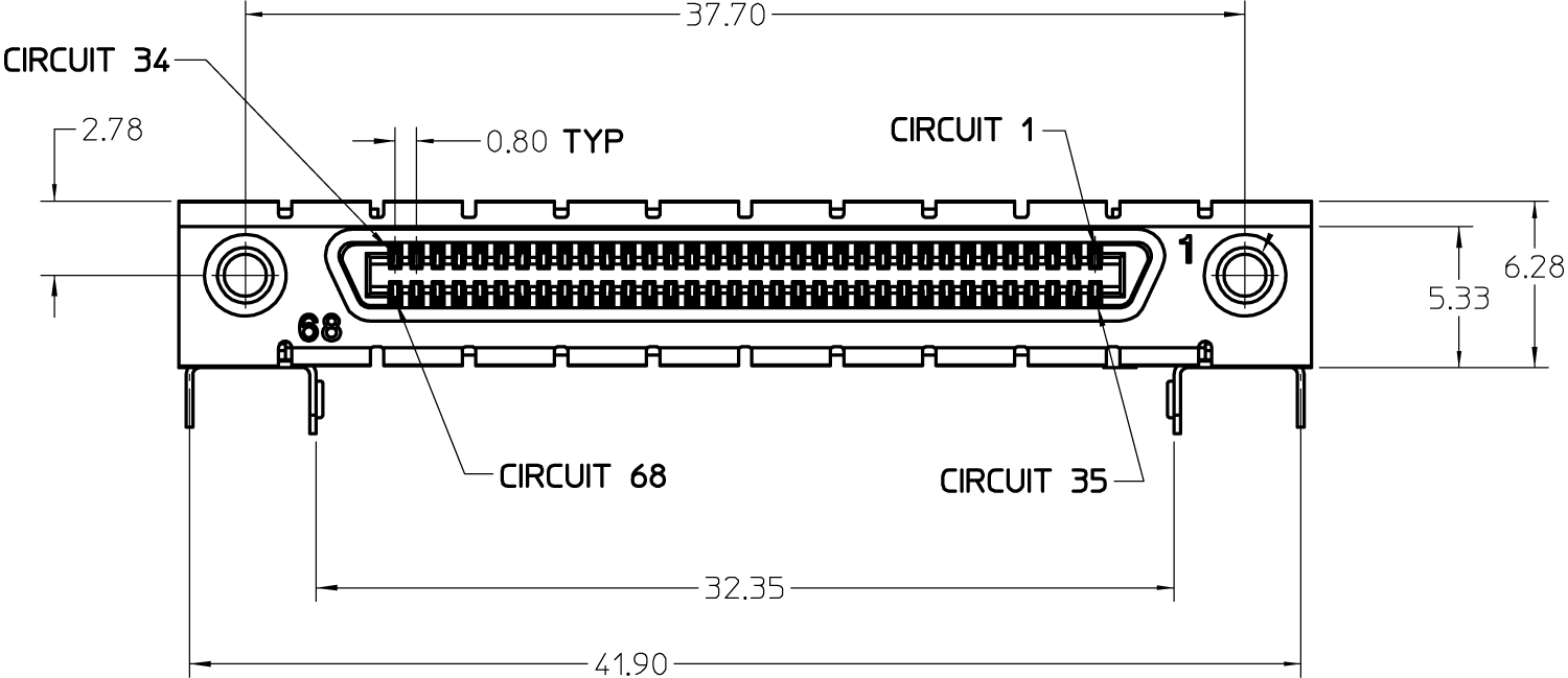
| ### DIO Port |
The DIO port is a VHDCI 68 pin connector as introduced by the SPI-3 document of the SCSI-3 specification. It is a female connector that requires a 32 mm wide male connector. The interface standard is switchable between LVDS (low-voltage differential signalling) and LVCMOS/LVTTL. The DIO port features 32 user-controlled bits that can all be configured byte-wise as inputs or outputs in LVCMOS/LVTTL mode, whereas in LVDS mode, half of the bits are always configured as inputs. For more specifics on how the user-definable pins can be set.
| Parameter | Details | Min | Typ | Max |
|---|---|---|---|---|
| supported DIO interface standards | - | LVCMOS/LVTTL (single-ended, 3.3 V); LVDS (differential) | ||
| high-level input voltage VIH | LVCMOS/LVTTL | 2.0 V | - | - |
| low-level input voltage VIL | LVCMOS/LVTTL | - | - | 0.8 V |
| high-level output voltage VOH | LVCMOS/LVTTL at IOH < 12 mA |
2.6 V | - | - |
| low-level output voltage VOL | LVCMOS/LVTTL at IOL < 12 mA |
- | - | 0.4 V |
| high-level output current IOH (sourcing) | LVCMOS/LVTTL | - | - | 12 mA |
| low-level output current IOL (sinking) | LVCMOS/LVTTL | - | - | 12 mA |
| input differential voltage VID | LVDS | 100 mV | - | 600 mV |
| input common-mode voltage VICM | LVDS | 0.3 V | - | 2.35 V |
| output differential voltage VOD | LVDS | 247 mV | - | 454 mV |
| output common-mode voltage VOCM | LVDS | 1.125 V | - | 1.375 V |
| Pin | Name | Description |
|---|---|---|
| 68 | unused | leave unconnected |
| 67 | unused | leave unconnected |
| 66 .. 59 | DIO[31:24] | digital input or output byte (set by user) |
| 58 .. 51 | DIO[23:16] | digital input or output byte (set by user) |
| 50 .. 43 | DIO[15:8] | digital input or output byte (set by user) |
| 42 .. 35 | DIO[7:0] | digital input or output byte (set by user) |
| 34 | GND | digital ground |
| 33 | unused | leave unconnected |
| 32 .. 1 | GND | digital ground |
| Pin | Name | Description |
|---|---|---|
| 68 | unused | leave unconnected |
| 67 | unused | leave unconnected |
| 66 .. 59 | DI+[31:24] | digital input byte |
| 58 .. 51 | DI+[23:16] | digital input byte |
| 50 .. 43 | DIO+[15:8] | digital input or output byte (set by user) |
| 42 .. 35 | DIO+[7:0] | digital input or output byte (set by user) |
| 34 | unused | leave unconnected |
| 33 | unused | leave unconnected |
| 32 .. 25 | DI–[31:24] | digital input byte |
| 24 .. 17 | DI–[23:16] | digital input byte |
| 16 .. 9 | DIO–[15:8] | digital input or output byte (set by user) |
| 8 .. 1 | DIO–[7:0] | digital input or output byte (set by user) |